| Name | Institution | |
| Frank Thompson | University of Manchester |
Manufacture of Printed Circuit Boards
Introduction
Although an initial electronic circuit may well be fabricated on Vero board as a prototype, it is preferable that printed circuit boards (PCBs) be used for the final construction of any electronic circuit. Indeed, circuits used in industry will inevitably use PCBs because they have good reliability and, if necessary, component placement on the boards can be automated.
In its simplest form a circuit will have copper tracks on the underside of a fibreglass reinforced board. Holes are then drilled through the board to take components which are connected to the copper tracks by soldering. This is illustrated in Figure 1.
With the increasing popularity of surface mounted components, the track is on the top surface and a full copper earth plane covers the bottom surface. Components are then soldered to pads on the upper surface.
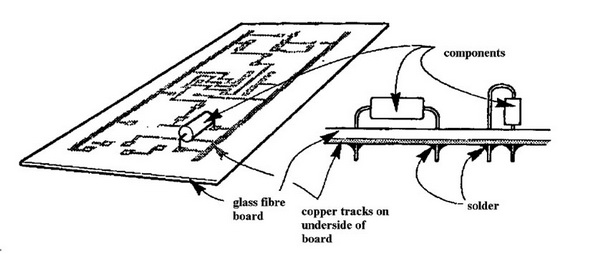
Figure 1. Diagram showing a single sided PCB with components added.
In cases where a circuit is likely to be popular, for instance, a waveform generator (based on the IC ICL 8038) component stockist (Farnell, Maplin, RS Components) will have already made a PCB to facilitate circuit construction. Other 'ready made' units may be purchased as 'evaluation boards'. For these circuits it will have been found that the track layout has a critical effect of the performance of the final circuit and hence chip manufacturers want to provide a full circuit to present their devices in the best possible light. In addition, it is often found that magazines serving the hobbyist market will provide art work suitable for making a PCB mask as shown in Figure 2.
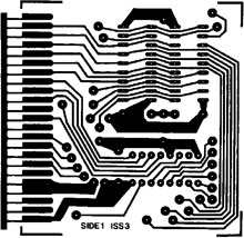
Figure 2. Mask to define photo-resist on the PCB board
Thus, we see that there may be a number of starting points in the fabrication of a circuit on a PCB but if it is assumed that the starting point is a schematic diagram then the processes which have to be addressed in the manufacture of a PCB are:
- (a) production of a mask to define the copper tracks - the 'artwork'
- (b) transfer of the image and subsequent board etching to produce the copper tracks.
The stages will now be considered using the example of a simple seven-segment display. (Note - if one intends to start at the very beginning, some useful tips are provided by Bill Sim of Aukland University)
Schematic Diagram
A very simple circuit, often used in schools, can be taken as an example for PCB production. The 4511 IC converts a binary input to decimal output which is then displayed on a seven-segment LED display. The schematic is given in Figure 3.
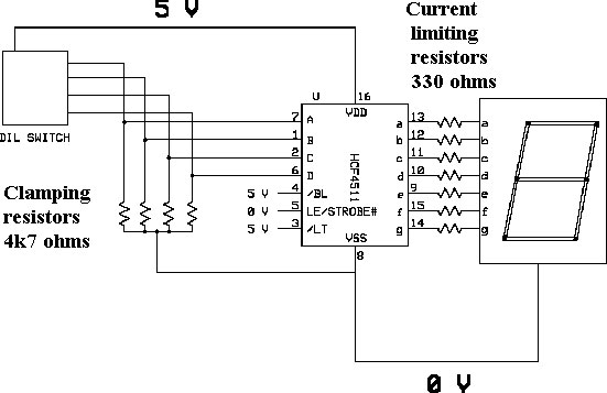
Figure 3. Schematic diagram for a simple seven-segment display
One must appreciate that even if the circuit looks relatively simple, circuit complexity in the 4511 is high.
Therefore, most of the hard work has already been accomplished by the IC manufacturers.
The above Schematic was drawn using Express.SCH and bit-mapped into Paint. Almost all drawing packages will allow drawings to be documented this way. Various types of board may be produced according to the complexity or functionality of the circuit. A typical double-sided board will require a mask for the underside of the board, a mask for the top side and a silk-screen layer to show the outline of the components and text to identify each of the components. Also, there will be added features regarding the drilling of holes for component placement or, in the case of surface mounted components the board may not require drilling. Thus, the boards may be listed as follows:-
- Non drilled boards
- Drilled boards
- Plated through hole boards
- Specialist circuits
- Duroid or ceramic based boards for microwave use
- Flexible printed circuits for many industrial components.
-
- Tracks are often screen printed on a flexible substrate and then laminated to avoid
exposing the track. The flexible material can, in fact, be the same material as used for
rigid boards ( source: San Francisco Circuits )
-
- Tracks are often screen printed on a flexible substrate and then laminated to avoid
The tracks on the board may simply be left as bare copper but this does tarnish with time. They can however be sprayed with a tin-based compound to aid soldering and prevent degradation of the board.
More usual for the professional board is to apply a solder masking process which adds a protective coating to the board and leaves small pads (solder dipped) for the attachment of components. Such a board is illustrated in Figure 4
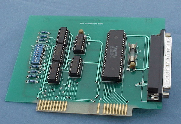
Figure 4. An interface board for a pre-2000 millennium PC
High cost option
There is no shortage of companies wishing to help you with your task of making a PCB. A Google search gives
several hundreds; San Francisco Circuits, Express PCB and Pad2Pad, to name a few.
Using PCB layout software, a mask can be made from a schematic and this is then checked. Fully drilled boards will then be produced in a matter of days after the order has been dispatched.
Low cost option
The following two pages were used by pupils in a school and could well be used in a home environment to produced PCBs at the other end of the cost scale.
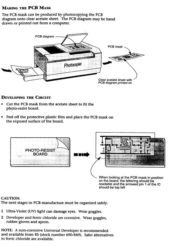
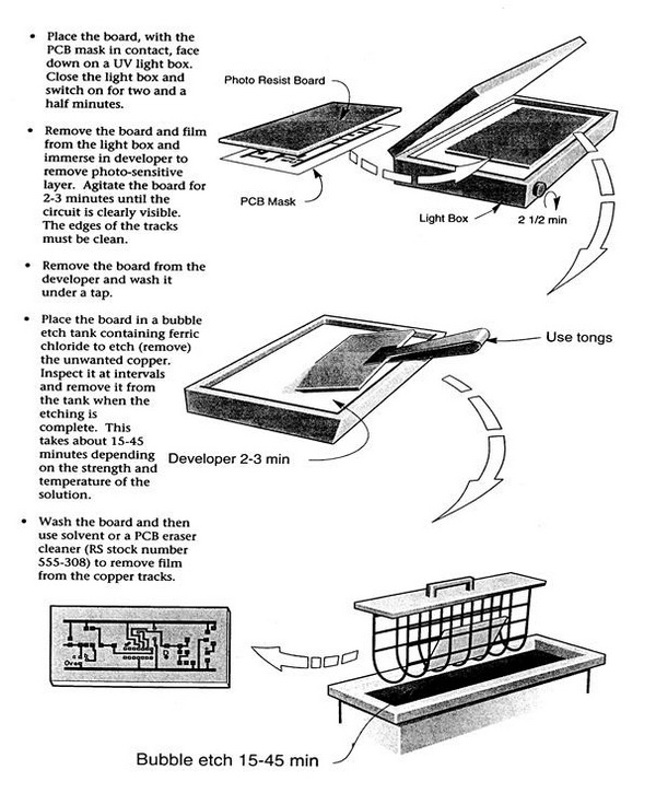
(All chemical and equipment from RS Components 'PCB Laboratory', purchase code 494 0889)
It is fair to say that only variable results were achieved by the above method and broken tracks were often reported. These are not difficult to repair but often escape notice until the trouble-shooting of a defective circuit.
Perhaps a better method is that suggested on web site www.fullnet.com where the printed image is transferred to a board by applying a hot iron normally used for pressing garments. The author has not tried this method but full details are provided in the article. Again, one is not short of advice when embarking on PCB fabrication; a Google search with 'homemade PCB' gives thousands of hits.
A general and very readable article regarding tips for laying out a PCB board on Alternate Zone has been given by D.L. Jones; and this I would recommend as essential reading before putting pads to paper.
Seven-segment display
The following PCB has been produced with school projects in mind and it must be stressed at this stage that a PCB suitable for school use will have a somewhat different appearance to that used in industry; ease of soldering is by far the most important aspect of the design. Therefore pads are enlarged and tracks are, typically, 50 thou. Also, tracks are less congested than would appear on a normal board. I have watched countless generations of pupils put off electronics for life by having very poor quality PCBs on which to add components. Through no fault of their own, pupils build a defective circuit and become disillusioned with this most important area of technology.
Several CAD packages are available for PCB layout - Pad2Pad, Express PCB, WinQcad, Eagle, PentaLogix, Protel to name but a few. Almost all CAD packages will auto-route from a schematic to a PCB board but, in the case of this simple seven-segment display board, the PCB was draughted manually. ExpressPCB (illustrated in Figure 5) is by far the easiest software to use but board manufacture is expensive.
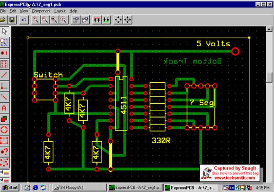
Figure 5. Partial-screen display for ExpressPCB artwork of seven-segment board
Since Protel 99SE was available in the Department this is the CAD package that was used to manufacture the display board. The board used was type FR4 with 1 oz copper. The .pcb file has been exported as a .doc file and is given in Figure 6
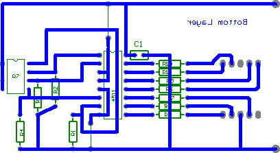
Figure 6. Layout from Protel 99SE
(note - a capacitor C1 has been added to the layout and the tracks are slightly different to that given in Figure 5)
- By using 'copy and paste', a pattern for multiple boards is produced (eight boards in the present case).
- The CAD package then generates Gerber files .gtl for top layout of board and .gbl for bottom layout of board (only .gbl was used on the present board). In addition, a drill file is produced .drl.
- A laser photo-plotter, type Cresent 30, produces positive or negative images from the Gerber files and the copper coated boards are drilled using a numerically controlled drilling machine, type Vero.
- The drilled boards are cleaned and dried and then laminated with a photosensitive film.
- The sensitised boards, with images (from Cresent 30) attached, are now exposed to UV light for 21 seconds - using two lamps both sides can be illuminated simultaneously.
- The development stage leaves the tracks covered and the rest of the copper clear. This will take, typically, slightly over one minute with fresh solution.
- Etching times are typically 5 to 6 minutes for 1oz copper boards but temperature, agitation and strength of solution are clearly important for etching times.
- After etching the resist film is stripped from the copper tracks by scrubbing and, after cleaning and drying the board can be tinned.
- Individual boards are then cut from the composite board by using a guillotine.
Figure 7 shows two boards - the top board has the components added and the bottom board shows the track side of the board as a copper finish.
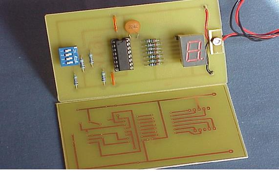
Figure 7. Finished boards for seven-segment display unit
The two yellow wires are 'crossovers' and, at vastly greater cost, could have been a 'top' Gerber file for a double-sided board. Application of a 5V supply to the board gave 0 display with the switches off and 1,2,4,8 for the respective switches 1,s2,3,4 - SUCCESS! A modest step for man and only a modest step for mankind. However, as confidence is gained the layout of more complex circuits can be attempted.
Moving up in the frequency world
Experience with high frequency circuits (frequencies above 1 GHz) can also be achieved with standard PCB boards with a track on the upper surface and a continuous layer of copper on the lower surface to produce a so called microstrip circuit. The design of such circuits has been greatly simplified by the introduction of simulation software packages (Agilent Design Systems, ADS, Ansoft Seranade, etc).
The lengths of the copper tracks are very important at these high frequencies but, with the design packages a circuit can be laid out and simulated S-parameters evaluated before any board is produced.
The following example is a Hybrid Ring circuit which is used for radar applications. The mean circumference of the ring is 1.5 λ, where λ is the microwave wavelength in the board material. Ports 3 and 4 have electrical distances of 0.25*λ and 0.5*λ from port 1. So, power incident on port 1 will give outputs at 3 and 2 since there will be no destructive interference but no power at 4 because the waves arrive 180° out of phase. Conversely, power incident at 4 will divide between 4 and 1 and give no power at 3. Thus, for radar the transmitter is attached to port 1 and an antenna is connected to port 2 then the receiver is connected to port 4 and a termination to port 3. During transmission no signal is produced at port 4 but a reflected signal coming to the antenna does produce an output at that port. Hence, a very sensitive receiver can be attached to this port to detect low level radar pulses. (Note: it will not be saturated by the transmit pulse because no power reaches port 4 in this 'forward' mode.)
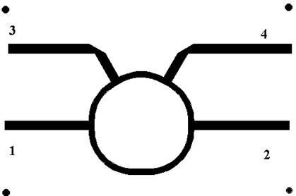
Figure 8. A microstrip Hybrid Ring circuit for Radar detection
(the spots just define the boundaries of the circuit)
Coaxial leads can be connected to the board using re-usable SMA to board clamps as illustrated in Figure 9.
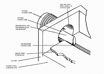
Figure 9. Coaxial to board clamps
The outer shell of the clamp is in good electrical contact with the earth plane by two fixing screws and it
is a simple matter to solder the inner pin onto the microstrip conductor.
A photograph is given in Figure 10 of the Hybrid Ring device. Also included is a detector circuit from Analog Devices and this detector operates with little degradation up to frequencies of 8 GHz.
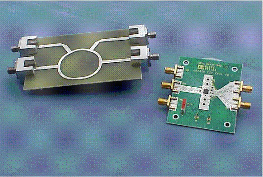
Figure 10. Hybrid Ring microstrip circuit (left) Analog Devices Board (right)
Further details of microstrip design are given by Dana Brady, High Frequency Electronics July 2002
Summary
The above article has given a description of PCB fabrication techniques using a seven-segment display circuit as an example. Additional web sites should help the beginner to undertake a simple design.
Brief details have been given for a microstrip circuit but these circuits require a fair degree of theoretical understanding of microwave engineering.
One final point must be stressed. The developments in IC technology have been totally overwhelming in the past decade; one need only look at the Intel web site. But ICs need to be placed on a PCB for power and interface connections. Therefore, the humble PCB, in my view, needs rather more recognition than it presently receives since, without it, electronic circuits, with all the sophistication that present ICs have to offer, would not be able to function.
Afterthoughts
After extolling PCBs in the article I do have to add a note of caution.
- My son in law has recently experienced a fault on a flexible PCB in his VW Polo car. Read more on this web site (link).
- I recently repaired a CD player which had an imperfect PCB.
- One of the Analogue Devices Evaluations Boards (I had to purchase THREE!), illustrated in Figure 10, is not functioning correctly.
I am sure that with better Quality Control such faults would not have occurred but perhaps I should close with a warning - a perfect world can never be assumed!!